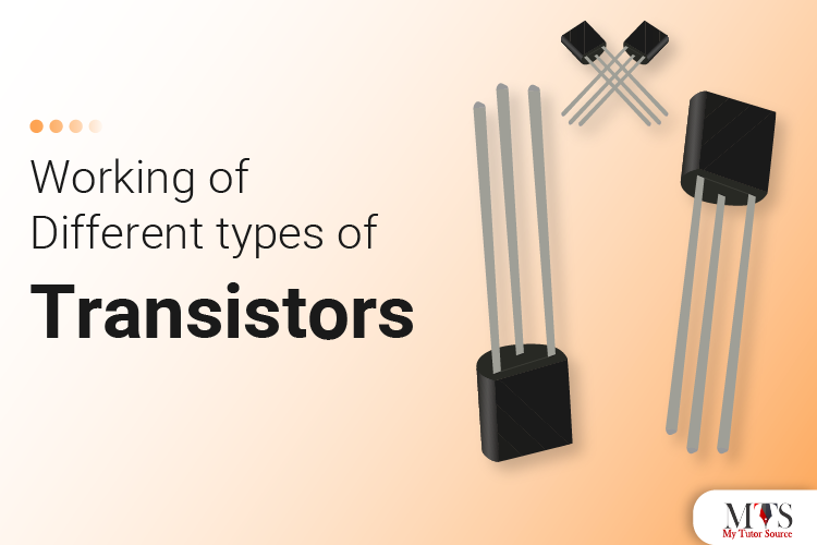
A transistor is a small device that can be used to serve two different purposes. In some situations, the transistor can be used as a switch, whereas in other situations, it can be used as an amplifier.
It can serve two-fold purposes in a way that it can be used to increase the flow of electricity or voltages, and it can be used to inhibit or turn off the flow of current.
Do you wish to learn about all the aspects of transistors in detail? Our private physics
tutor can guide you thoroughly to gain all the knowledge of the subject.
Here we have discussed the different uses and applications of transistors based on their modes of working.
What is a Transistor
A transistor is mainly considered as a semiconductor device because it can be used as both; an electrical conductor and an inhibitor. The two main purposes of a transistor are either working as an amplifier or a switch in the circuit. There are basically three main terminals of a transistor that makes it function properly. The three terminals include base, emitter, and collector. Based on the usage and functioning of a transistor, there are two ways a transistor can be used, including:
Let’s discuss how the functioning of a transistor differs while functioning as an amplifier and a circuit.
Configuration of a Transistor
Here the working of a transistor is based on the configuration of the circuit. Different configurations determine different workings of a transistor. There can be three ways through which the transistor configuration can occur, including:
- Common base
- Common emitter
- Common collector
Two terminals work for input and two terminals for output. In this situation, the third terminal is usually taken as a common terminal for both input and output; the configuration changes based on the common terminal that has been taken.
Common base
If the transistor is working with the common base configuration, it means that the base terminal has been used as a common terminal for input and output. At the same time, the other two terminals work individually for the input and output.
In this way, the base here provides two folded functions, i.e., for the input and the output of voltages at the same time. This is why base in this situation is known as a common base.
Common emitter
When the working of a transistor is in a way that the emitter is taken as a common terminal for both input and output while the two other terminals work separately for the input and output, then the configuration is named as a common emitter.
Here the emitter is being used to provide the working of both the input and output voltages at the same time. This is why it is known as a common emitter.

Common collector
If the transistor is working with the collector terminal as a common terminal for both; input and output, then while the two other terminals are working individually for input and output, then the configuration is named as a common collector.
In this situation, this collector is giving a purpose of both the input and the output voltages at the same time. In this way, this terminal is known as the common collector.
Transistors as amplifiers
When a transistor is working as an amplifier, it tends to increase the current by changing a weak signal into a strong one. When we are using a transistor in the form of an amplifier, then it is used for the conversion or amplification of a weak signal from the input to a strong one at the output. By using the transistor as an amplifier, the input signal with a rather low value is converted into an output signal with a higher value.
The main purpose of using amplifier transistors is to enhance the signal quality to increase the work effectiveness of the circuit. This property of a transistor is quite helpful in the working of radio signals or distant communication workings.
Active region
This region comes in between the saturation and cut-ff region. While operating in the active region, the transistor is usually working as an amplifier. In this region, the base-emitter junction is found to be in the reverse bias, whereas the base-collector junction is found to be in the forward bias. Just like the switching property of the transistor happens in the saturation or cut-off region, the amplification by the transistors usually occurs when the transistor is present in the active region.
An example of amplified current
Let’s discuss through an example how a small amount of voltage can have a large impact on the output voltage hence amplifying the output voltages.
If a small amount of voltage like 0.2V has been applied to the emitter, this will eventually produce a current of 2 mAmp in the emitter. This will lead to an increase in the voltages that are being collected as output voltages.
With this voltage and current, there would be a resistance of some extent like 5 kΩ
Since V=IR
We can say that,
5 x 2= 10V
From this example, we can conclude that a small input voltage that was 0.2v created a larger output voltage effect that was 10v.
In this way, the smaller voltage was amplified into a larger voltage amount by the use of a transistor.
Transistors as switches
If a transistor is working as a switch, it means that a small amount of current in the circuit will be turned into a larger amount of current, having a major impact. The working of the transistor as a switch will determine whether the current is flowing or not. In other words, it determines if the circuit is open (OFF) or is it closed (ON).
When working as a switch, the transistor operates in two main regions, including the cut-off region and the saturation region.
Cut-off region
A transistor as a switch is responsible for determining whether the circuit is open or closed. When there is zero current present at the emitter, there will be zero current at the collector; hence the switch will be considered as an open switch or off mode. When the switch is open, the transistor is working in the cut-off region.
Since the circuit is open when the transistor is in the cut-off region, there is no current flowing through the circuit; hence the circuit will be considered in OFF mode. In this way, the transistor in this region is used as a switch.
Saturation region
On the other hand, when a certain amount of voltage, usually greater than 0.7V, is applied to the base terminal, then there is a flow of current at the collector terminal. In this situation, the circuit is closed and in ON mode. When the circuit is closed, the transistor is said to be working in the saturation region. In the saturation region, there is the voltage, and current is maximum at the base and the collector terminal.
Since the circuit is closed when the transistor is present in the saturation region, there is maximum current flowing through the circuit because of the voltages that are coming from the source. In this way, the circuit is said to be turned ON with current flowing through it. In this way, the transistor is used as a switch when present in this region.
Terminals of transistors
There are three main terminals of a transistor that work together for the normal functioning of the transistors and transfer the charge from one part of the circuit to the other. Let’s discuss the working of the three terminals of a transistor.
Emitter
This is the first terminal of the transistor with a moderate size. Being located at the beginning of the transistor, the emitter is mainly responsible for transferring the charge to the collector through the base terminal. Since it is responsible for supplying the charge, it is connected to the base via the forward bias. The charges are transferred to the base terminal via the junction present between the emitter and base.
Base
This is the second terminal on the resistor. There are two junctions at the base terminal. One that connects the base with the emitter is known as the input junction, and the other that connects the base to the collector is known as the output junction. The input junction is in a forward bias, whereas the output junction is in a reverse bias.
The base is located in the middle region of the transistor with a relatively small size in comparison to the emitter and the collector region.
Collector
This is the final terminal of the transistor. It is located at the end of it, and the size is relatively larger than both terminals, i.e., base and emitter. The large size of this terminal is for collection purposes as the charges sent from the emitter via base are supposed to be collected in this region.
There is a reverse-biased junction present here that connects the base with the collector.
Types of transistors
Based on the configuration and material of the terminals, there are two main types of transistors that are further subdivided into other categories.
The two main types of a transistor are:
- Bipolar junction transistor
- Field-effect transistor
The bipolar junction transistor (BJP) is further divided into two other configurations that are PNP and NPN, whereas the field-effect transistor (FET) further has two more configurations that are JFET and MOSFET.
Let’s discuss how these configurations and their uses distinguish the different types of the transistor from each other.
Bipolar junction transistor (BJT)
The bipolar junction transistors are the ones that contain two junctions of either P or N material. Here the N is supposed to indicate the negatively charged material present in the transistor, whereas the P would indicate the positively charged material.
The BJP transistor has further two types of configurations that bring the differences in the functioning of a transistor, including:
NPN
The NPN transistor is the one that has the configuration in a way that the P material is situated in the middle of the N material. There are three terminals in the NPN transistor, i.e., the emitter, base, and the collector, where the base is connected to the emitter via the forward bias and to the collector via the reverse bias.
The flow of electrons in the NPN configuration is from the emitter to the collector since the two ends are both equipped with negative material.
Working
In the NPN transistor, when there is no voltage being applied, then the transistor is said to be unbiased. When voltages are being applied, there is a flow of charge that generates the current in the circuit. Since the left and right sides of NPN transistors are negative material, it is known that the majority of charge carriers in these two regions are negatively charged electrons, whereas the middle region (base) that is made of P material has majority carriers as holds which are positively charged ions.
In this way, the flow of charges in this transistor is from emitter to base, which is then transferred to the collector.
PNP
The PNP transistor, on the other hand, is the one with the opposite configuration. The N material in this transistor is placed between the P materials on both sides. In this transistor, the electrons are taken from the base that is present in the middle. When the current comes in the base, it is then further sent to the collector, where it is amplified.
This transistor has two PN junctions. These are formed when the emitter is connected to the base forming one PN junction, and the other is formed when the base is connected to the collector forming another PN junction.
Working
If there is no voltage being applied to the given transistor, then it is said to be an unbiased PNP transistor. After the application of voltage, there is a flow of charges that generate the current. In the case of a PNP transistor, the P region is constituted of holes as their majority charge carrier, and the negatively charged electrons are considered as the minority charge carriers. Whereas, in the base that is N material, the electrons are considered as majority charge carriers, and the holes are considered as minority charge carriers.
In this way, the major overall charge carriers in the PNP transistor are the holes instead of the negatively charged electrons.
The preference of NPN over PNP
Usually, in electric circuits, the NPN transistors are preferred more over the PNP transistors. Although the major difference between both transistors is the configuration of the P and N material, this changes the mode of operation for both transistors.
Here are some reasons why NPN transistors are preferred more over the PNP ones:
Electrons movement
The majority carriers in the NPN transistors are the negatively charged electrons, and it is known that electrons have a higher mobility rate and travel faster in comparison to the holes present as majority carriers in the PNP transistors. Being positively charged ions, they are less mobile than the electrons.
The higher mobility of the electron allows more electricity conduction in the given circuit, which makes NPN a more preferred transistor over the PNP one.
Grounding the negative terminal
Grounding the negative terminal helps to keep the balance in the flow of current and to minimize the unbalanced current flow. The NPN has a more prominent negative field which helps to easily ground the negative terminal, whereas the PNP transistor has a positive field being more prominent. This inhibits the prominent negative exposure of the transistor and inhibits the ease of grounding the negative terminal.
In this way, the NPN transistor is preferred more over the PNP so that the negative terminal can be grounded in an easy way.
NPN transistor as switches
When the transistor is being used as a switch, the NPN transistor works more efficiently in comparison to the PNP transistor. The power of switching is more when the working configuration of the transistor in NPN with more negative field instead of the PNP transistor with a positive field. Similarly, the frequency rate of the NPN transistor is better than PNP, which makes the amplification output rather better than the PNP configuration.
The switching speed and the amplification rate both are higher in the NPN transistor. Hence both modes of a common transistor work better when the configuration is done with P material being centered with the N material. Rather than having the opposite configuration, that is the PNP.
Costing benefits
The manufacturing and production cost of an NPN transistor is quite less in comparison to the PNP transistor. To limit the cost of transistor manufacturing, the NPN transistor is used more commonly than the PNP transistor.
More reliable
Being smaller in size and with low production cost, the NPN transistor is considered rather more efficient and reliable than the PNP transistor.
Field effect transistor
This is the type of unipolar transistor that does not have double junctions like the BJT transistor. Being unipolar, the FET transistor either has P material or N material embedded in it and because of this, there are either electrons or holes working as the charge carriers in this transistor. Both charge carriers won’t be presented at the same time in FET.
FET is known to have a high input impedance which makes it perfect to be used in an integrated circuit.
FET is considered as a voltage-controlled device as its functioning depends on the output voltages that are provided to it by the input voltages. There are three different terminals of the FET which are different from that of the BJT. these three terminals are:
Let’s discuss how the placement and roles of these terminals are important for the normal functioning of FET.
Gate
This is the terminal that is mainly responsible for the flow of charge carriers in the transistor. It is made by the diffusion of an N-type semiconductor and a P-type semiconductor. It is placed close to the channel so that it can ensure that the charge carriers are flowing in the right way from the source to the drain.
Source
This is the terminal of the FET where the electrons or holes enter the circuit channel to travel further towards the drain for the normal functioning of the circuit. The entrance of charge carriers here is controlled by the gate.
Drain
This is the final terminal in the FET where the incoming charge carriers are exited from. The electrons basically enter the channel from the gate and exit from the drain; this flow of charge carriers from the source to the drain is controlled and regulated by the third terminal that is the gate.
Based on the working of this transistor, there are two different types of FET transistor as discussed below:
JFET
The junction field-effect transistor (JFET) is a type of FET that is usually used as a switch in a circuit. JFET is a voltage-controlled device and works with either the P-type material or the N-type material. Based on this configuration, the JFET is further divided into n-type JFET and P-type JFET.
Since it is controlled by the voltages provided to it when there is no voltage provided to it, the transistor is considered to be in an ON state, and when there is a supply of voltages, the transistor allows a limited amount of current to flow through the circuit.
If the P-type material is the main constituent in the JFET, then it is known as the P-type JFET, and the main charge carriers in this transistor are the positively charged ions that are the holes.
On the other hand, if the main constituent of the transistor is the N-type material, then it is known as the N type JFET, and the negatively charged electrons are the main charge carriers in it.
Metal oxide semiconductor field effect transistor (MOSFET)
MOSFET is a type of Field effect transistor that is mainly used for amplification or switching purposes in a given circuit. This is also a voltage-controlled device, as the small amount of voltage brings changes in the current flow of the circuit.
The MOSFET further has two types of configurations that are the depletion type and the enhancement type.
If the MOSFET is the depletion type, then it means it is in the close switch form, and in order to turn off the switch, there needs to be source gate voltage provided.
On the other hand, if this transistor is an enhancement type, it is considered to be in an open switch form, and to turn on the switch, there should be source gate voltages.
Difference between JFET and MOSFET
There are a few differences between the JFET and MOSFET, as discussed below:
- The JFET works only when present in the depletion mode, which means it works in a close switch form, whereas MOSFET works in both modes, whether in depletion mode or enhancement mode.
- The conductivity in the JFET is usually affected by the reverse biasing in the channel, whereas in the MOSFET, the conductivity is affected by the carries that are present in the channel.
- The resistance offered in the drain terminal of JFET is rather high than the drain resistance in the MOSFET.
- When it comes to the manufacturing process, the process is rather simple for the JFET but a bit complex for the MOSFET.
- The JFET is considered as the transistor with three terminals, whereas the MOSFET is considered as the transistor having four terminals.
The uses and applications of transistors
There are several uses of transistors in our daily lives. Some of them have been discussed here as follows.
- Transistors can be used to serve two major functions either the switching of the circuit or the amplification of current in a given device.
- As a switch, transistors are used in digital and analog circuits as well.
- When a greater amount of current is required, the bipolar junction transistors can come to work by amplifying the current that passes through the base of it.
- Transistors are used widely in the production of our mobile phones. The transistors present in mobile phones are responsible for storing and regulating current flow and also amplifying the signals that are coming to the mobile phone.
- Integrated circuits are embedded in many of our daily life devices. These small units are responsible for transmitting electrical signals from one place to another via other units that mainly includes the use of transistors. Transistors are the main functioning units of these microchips that are known as integrated circuits.
- All the electric devices are providing sound functions, including the radio, cell phones, or the computer use transistors to amplify the sounds from the device and hence enhancing the quality of the sound.
Advantages and disadvantages of using a transistor
Just like everything else, there are several advantages and some disadvantages associated with the use of a transistor. Some of them have been discussed below:
Advantages
Some of the advantages of using a transistor have been discussed below.
- The many advantages of a transistor are because of its very small size and less manufacturing cost. A transistor is rather small in size and provides the work efficiently by occupying very little space in a device.
- It can act as an insulator and a conductor both. This is why it is sometimes referred to as a semiconductor. When there is a need for a flow of current, the transistor acts as a conductor, whereas when the current flow needs to be stopped or reduced, the transistor acts as an insulator.
- When a transistor is being used as a bipolar junction transistor, it allows the flow of positive and negative charge carriers at the same time. There are negative and positive charges flowing across in the form of electrons and holes, respectively.
- With a low production cost, small transistors can be used to manufacture a rather large size of integrated circuit.
- Transistors are quite reliable because of their small size and less sensitivity to mechanical exposure; because of this, there are lesser chances of physical damage to the equipment.
- The use of silicon in the transistors is essential in the devices that work in the higher current environment. AC devices that require the working of higher current levels can work right with BJ transistors made up of silicon base.
- It does not require a large number of voltages for a large amount of voltage output. In this way, the transistor offers large voltages with the input of a small number of voltages.
- There is no noise related to the working of a transistor providing noiseless operations. Being so small in size, there is no moving element in the equipment of a transistor which helps to avoid the wear and tear situation of a machine.
Disadvantages
With many advantages associated with the use of transistors, there are some disadvantages as well. Some of the disadvantages have been discussed below:
- Higher voltages and current can have a bad effect on the quality of a transistor. It should be placed where the voltages and current levels are relatively higher.
- In the case of reversing voltages, transistors usually fail to work, so they should be used with care when operating in an AC device so that the reverse voltages would not destroy the working of the transistor.
- Transistors are rather sensitive to the application of temperature. If there are higher levels of temperature being applied to the device, it can eventually damage the transistor.
- The small size of a transistor can be a drawback of it as well. If there is circuit damage or particularly in the transistor, the repairing process is rather difficult due to its small size.
Conclusion
Transistors are very small devices that are installed in a circuit and can be used to perform many functions, including the amplification of the current or the voltage and the switching on and off of a given circuit. The transistor has three main components that make the transistor work normally, including the emitter, base, and collector, whereas in some types of transistors, the three terminals include the gate, drain, and source.
There are two types of charge carriers flowing in a transistor that makes the current flow, including the negatively charged ion that are electrons and the positively charged ions that are the holes.
If you wish to study the detailed aspects of the transistor and related elements, learn all about it from our private home tutors.
Find Top Tutors in Your Area
Find A Tutor